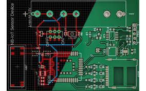
Introduction to Silk Screen in PCB Manufacturing
Silk screen, often referred to in PCB manufacturing as the silk-screening process, involves the application of text and symbols onto a printed circuit board (PCB). This method is crucial for providing essential information such as component locations, polarity indications, warning symbols, and company logos directly on the PCB surface. It serves not only as a functional element but also as a branding tool for manufacturers.
Key Functions of Silk Screen on PCBs
The primary role of the silk screen process in PCBs is to facilitate easier assembly and troubleshooting. Here are some of the vital functions it performs:
- Identification: Silk screening helps in labeling components, test points, and other essential elements on the PCB. This is crucial during both the assembly and maintenance phases. It ensures that components are correctly placed according to the circuit design.
- Instructions: Many PCBs include operational or warning instructions directly on their surface. Silk screening can apply these vital instructions, which can range from simple operation guidelines to safety warnings.
- Enhanced Usability: By marking pin numbers around microcontrollers or other multi-legged components, silk screening makes it easier for technicians to identify connections quickly, enhancing the usability of the PCB.

Technological Advancements and Precision
Recent advancements in PCB manufacturing technology have greatly improved the precision and clarity of silk screening. Traditional methods involved manual screen-printing, which was prone to human error and limited in resolution. Today, most manufacturers use digital or photo-imaging techniques that allow for much higher detail and consistency in text and images.
Material Considerations
The ink used in the silk-screening process is typically a non-conductive epoxy ink. The choice of ink is crucial, as it must withstand the thermal stresses of PCB operation without degrading. Most PCBs require inks that can endure temperatures up to 280-300 degrees Fahrenheit during soldering processes. The durability and legibility of the silk-screened labels are tested under these conditions to ensure long-term reliability.
Challenges in Silk Screening
Despite its advantages, silk screening on PCBs faces several challenges:
- Space Limitations: As PCBs become smaller, fitting clear and legible text onto the board becomes increasingly difficult. This requires even more precise printing techniques and finer inks.
- Environmental Considerations: The inks used in silk screening must not only be durable but also compliant with environmental regulations such as RoHS (Restriction of Hazardous Substances).
Conclusion: The Impact of Silk Screen on PCB Efficiency and Functionality
Silk screen on PCBs plays an indispensable role in ensuring that each board functions as intended while adhering to safety and operational standards. The evolution of printing technologies has enabled finer, more durable markings, which are critical in the increasingly complex electronics industry. Silk screening remains a testament to how even traditional techniques can evolve to meet modern demands, blending functionality with precision in electronic manufacturing.